StudentShare
Contact Us
Sign In / Sign Up for FREE
Search
Go to advanced search...
Free

Electrical and Electronic Engineering laboratory logbook and report - Essay Example

Cite this document
Summary
The experiments described in this laboratory report “ELECTRICAL AND ELECTRONIC ENGINEERING LABORATORY LOGBOOK AND REPORT” detail the types and characteristics of bipolar junction transistors (BJT). It is divided into two sections: familiarization with transistors and common emitter transistor. …
Download full paper File format: .doc, available for editing
GRAB THE BEST PAPER92.2% of users find it useful
Electrical and Electronic Engineering laboratory logbook and report
Read Text Preview

Extract of sample "Electrical and Electronic Engineering laboratory logbook and report"

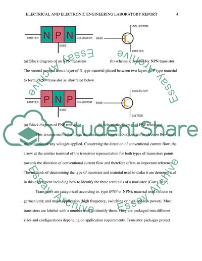
? ELECTRICAL AND ELECTRONIC ENGINEERING LABORATORY LOGBOOK AND REPORT By Date Abstract The experiments described in this laboratory report detail the types and characteristics of bipolar junction transistors (BJT). This report is divided into two sections: familiarization with transistors and common emitter transistor. The purpose of these experiments was to familiarize with two basic forms of transistors (the NPN and the PNP) and measure the base, emitter and collector currents for each form of transistor. We also carried out an investigation of the basic bias connections for a transistor. These steps help to familiarize with the basic measurements needed to characterize the properties of transistors. Secondly, we explore the output characteristics of a common-emitter transistor such as load line and operating point and their significance to the operation of a transistor. This laboratory report describes the theory of transistors, methodology used during the experiments, an analysis of the results collected, discussion and conclusion. Background Transistors are three-terminal devices made up of two semiconductor junctions similar to two junction diodes. These devices are made of either germanium (Ge) or silicon (Si). The basic structure of a transistor comprises two layers of n-type material with a layer of p-type material in between (NPN), or two layers of p-type material with a layer of n-type material between them (PNP). In both cases, the layer at the center forms the base of the transistor, whereas the two external layers form the emitter and the collector of the transistor (Gates 2012). The first method involves the P-type material sandwiched between two N-type materials as shown in the diagram below. (a) Block diagram of an NPN transistor (b) schematic symbol for NPN transistor The second method uses a layer of N-type material placed between two layers of P-type material to form a PNP transistor as illustrated below. (a) Block diagram of PNP transistor. (b) Schematic diagram of PNP transistor. This arrangement determines the direction of conventional current or electron flow and the polarities of any voltages applied. Concerning the direction of conventional current flow, the arrow at the emitter terminal of the transistor representation for both types of transistors points towards the direction of conventional current flow and therefore offers an important reference. The methods of determining the type of transistor and material used to make it are demonstrated in this experiment including how to identify the three terminals of a transistor (Gates 2012). Transistors are categorized according to: type (PNP or NPN); material used (silicon or germanium); and major application (high frequency, switching or high and low power). Most transistors are labeled with a number used to identify them. They are packaged into different sizes and configurations depending on application requirements. Transistor packages protect them, provide a means of making electrical connections to the three terminals, and act as heat sinks preventing heat damage. (Kal 2003)) Transistor packages The relationship between the currents and the voltages related to a transistor under different conditions of operation determine its performance. These relationships are collectively known as the characteristics of the transistors. These characteristics are published by the manufacturer of a particular transistor in a specification sheet that accompanies the device when purchased. One of the objectives of this laboratory experiment is to experimentally measure these characteristics of transistors and compare them to their published values (Kal 2003). A transistor acts as an amplifier; the basic function of the device is to switch a signal or to provide current amplification of the signal. For this purpose to be achieved, the transistor must be correctly biased by external voltages so that the base, emitter, and collector terminals interact in the appropriate manner (Kal 2003). In normal operation, the emitter-base junction of a transistor is forward-biased and acts in a similar manner to an independent diode while the collector-base junction is reverse-biased and typically does not pass any current. However, if the emitter-base junction is conducting forward current, it influences the reverse-biased junction causing it to pass a nearly equal quantity of much reverse current. The circuit diagram for a properly biased transistor is shown in the diagram below (Neamen 2001). (Kal 2003) During circuit operation, electrons are caused to flow from the emitter junction of NPN transistors by a forward bias. Forward biasing is the supply of a positive voltage on the base terminal with respect to the emitter terminal causing electron flow from the emitter. The electrons flowing towards the base terminal are influenced by the positive voltage applied at the collector terminal. Most of the electrons are attracted to the collector into the positive terminal of the reverse-biased voltage source while a few are absorbed into the base terminal which must be made very thin for this to occur. For a properly biased PNP transistor, the terminals of the battery must be reversed (Sedra & Smith 2004). The ratio of collector current to base current is called hfb. Since collector current is almost equal to emitter current, hfb ? 1. Therefore the ratio IC/IE= hfb ? 1. The ratio IC/IB is called hfe, therefore IB + IC = IE = IC/ hfb Therefore IC(1/ hfb-1) = IB And hfe = IC/IB = Therefore if hfb = 0.99, hfe = 0.99/0.01 = 99. In the common emitter bias mode of a transistor using an NPN transistor, the base current is derived from an input signal and the collector current is used to generate an output. The ratio hfe = IC/IB represents the transistor’s gain in terms if currents. i.e. hfe = (output current)/(input current) = current gain. Laboratory Methodology Transistor Familiarization Equipment 1 Electricity and electronics constructor EEC470. 1 Basic electricity and electronics kit EEC471-2. 2 multimeters or 1 microammeter, 100mA dc 1 power supply unit +5V variable dc, regulated and 1 voltmeter, 3 V dc. Procedure 1. The transistors BC107 and BC212 were selected from the EEC471-2 kit. The assortment of transistors selected is shown in the diagrams below. The terminals of the transistors in the kit were correctly identified. 2. The circuit for measuring transistor currents was constructed as shown in the figure below using a BC107-NPN transistor. A capacitor was used to ensure the circuit is stable and measurements are not affected. 3. The potentiometer was set to 0 (anticlockwise) and both power supplies switched on. 4. The VEB voltage was slowly increased by turning the potentiometer clockwise until IC began flowing .the voltmeter was connected temporarily between the emitter and the base on the transistor and the value of VEB recorded. 5. The voltmeter was removed and the VEB increased until the collector current almost equals 1 mA. The values of IC and IB were recorded in the table. The Common Emitter Equipment 1 Electricity and electronics constructor EEC470. 1 Basic electricity and electronics kit EEC471-2. 3 multimeters or 1 microammeter, 100 microampere dc 1 power supply unit 0 to 20 volts variable dc, regulated and 5V dc regulated. 1 milliammeter, 10 mA dc. 1 high resistance voltmeter, 10 V dc. Procedure 1. The equipment was set up as shown in the diagram below (figure1). 2. To find how the base current and VCE control the collector current, the circuit was set up as shown if figure 2. 3. VCE was set to 0.5V, and then the potentiometer was used to adjust the value of base current to each value given in the table. 4. The values of IC was recorded at each setting in the appropriate column and then repeated for all the values of VCE. On a graph, the values of IC were plotted against VCE for each value of base current. This graph represents the output characteristics of the transistor. Figure 1. Figure 2. Results and Discussion Transistor Familiarization Results The measurements made on the BC107 transistor used a circuit in which C and E terminals were biased with voltages relative to the base. The circuit is therefore referred to as a common base connection. The junctions can also be biased with voltages relative to the collector of emitter, to give common collector and common emitter connections respectively. Bias arrangements for NPN transistor The common-emitter bias arrangement has VCE greater than VBE to ensure that the collector-base junction remains reverse-biased. In the common-collector arrangement, VEC is greater than VBC to ensure that the emitter-base junction is forward biased. The three bias arrangements have significant differences with regard to their response to inputs. The common-collector and common-emitter circuits are the most important arrangements because the common-base is only used in special cases. The base current is much less than the collector and emitter currents; and the two are almost equal. The results from the table show that hfb decreases as IC increases while hfe increases as IC increases. In the arrangement below, a common-base biased transistor has the current values IB = 5µA and IE= 1mA. The collector bias current is calculated as: IC = IE –IB = 1mA - 5µA = 0.995 mA. hfb = 0.995/1 = 0.995 hfe = 0.995/0.005 = 199 Common Emitter Transistor Results: Output characteristics of common emitter transistor bias arrangement. IC is almost totally controlled by IB, but is not significantly affected by VCE. The output circuit represents a constant current source which may be passed into a load resistor to generate a voltage. The circuit formed represents a load line. Conclusion The objective of this experiment which was to familiarize with transistors was successfully achieved. The various characteristics of transistors were investigated and the common emitter transistor bias arrangement discussed in detail. The effect of applying voltage to different transistor terminals was also verified and results from the experiment recorded. The results were used to calculate values of transistor parameters and graphs plotted to show the behavior of a transistor under different conditions. In general, the experimental goals were successfully accomplished. Reference list Gates, E. D. (2012). Introduction to electronics. Clifton Park, NY, Delmar Cengage Learning. Kal, S. (2003). Basic electronics: devices, circuits and IT fundamentals. New Delhi, Prentice-Hall of India. Neamen, D. A. (2001). Electronic circuit analysis and design. Boston, McGraw-Hill. Sedra, A. S., & Smith, K. C. (2004). Microelectronic circuits. New York [u.a.], Oxford Univ. Press. Read More
Cite this document
  • APA
  • MLA
  • CHICAGO
(“Electrical and Electronic Engineering laboratory logbook and report Essay”, n.d.)
Retrieved de https://studentshare.org/engineering-and-construction/1495779-electrical-and-electronic-engineering-laboratory-logbook-and-report
(Electrical and Electronic Engineering Laboratory Logbook and Report Essay)
https://studentshare.org/engineering-and-construction/1495779-electrical-and-electronic-engineering-laboratory-logbook-and-report.
“Electrical and Electronic Engineering Laboratory Logbook and Report Essay”, n.d. https://studentshare.org/engineering-and-construction/1495779-electrical-and-electronic-engineering-laboratory-logbook-and-report.
  • Cited: 5 times

CHECK THESE SAMPLES OF Electrical and Electronic Engineering laboratory logbook and report

Engineering System Safety Report about Microwave Oven

nbsp;More and more families are acquiring modern and complex household electronic and electrical gadgets to make their lives easier.... This section is composed of an electronic timer in addition to other protection and interlocking devices.... This paper talks about microwave oven which is one of the modern day household appliances that make life easier, faster and more convenient for humans....
12 Pages (3000 words) Book Report/Review

Electrical circuits

In The report looks deeper into the literature review of electrical circuits and electronic components.... The report outline drifts into determining the values by elaborating on the procedures followed in the methodology.... electronic components in electrical circuits include semiconductor devices diode, op amp and transistors.... The electronic component features are explained in developed electrical networks.... Signal systems make use of electronic...
15 Pages (3750 words) Lab Report

Electrical and Electronic Principles (A) UFMFP8-15-1

The purpose of this paper “electrical and electronic Principles (A) UFMFP8-15-1” is to experience and study the Kirchhoff's Voltage and Current Laws and to examine the given resistive circuits using the above laws and series parallel combinations of electronic circuits....  electrical and electronic Principles (A) UFMFP8-15-1 Aims and ObjectivesThe purpose of this lab is to experience and study the Kirchhoff's Voltage and Current Laws.... observations, results and comments) in your logbook as you carry out the complete task....
1 Pages (250 words) Lab Report

Electrical and Electronic principles

You are required to record all activities (observations, results and comments) in your logbook as you Aims and Objectives The purpose of this lab is to experience and study the transient behaviour of capacitors (charging and recharging of a capacitor networks) and also to examine simple electronic circuits containing parallel/series combinations of capacitors.... You are required to record all activities (observations, results and comments) in your logbook as you perform the simulation....
2 Pages (500 words) Lab Report

Electronic Laboratory Practise

In this report, a digital multimeter was used in taking current and resistance readings respectively.... hellip; It was noted that useful electronic applications such as a potential divider and current divider were also demonstrated.... The potential divider and the current divider which are critical components of electrical circuits were demonstrated.... Error estimation was also described in some cases and the impact it has especially in understanding electrical circuits....
2 Pages (500 words) Lab Report

Basic electric circuits and measurements

From this, the experiment is able to explain the relationship occurring between the… Intuitively, the nature of the experiment is guided by ohm's law which asserts that the amount of voltage flowing from one point to another end in a conductor is directly proportional to the current between the two points, while the Basic electric circuit and measurement The major objective of this lab report is to explore the aspect of electrical resistance of materials....
1 Pages (250 words) Lab Report

Electric Cart Deign

In the report, there will also be a parts list that will outline all components and the number of these components that will be used in the design of the electric cart.... This report's deliverables will be a minimum of three concepts generated and presented in a sketch form to represent the electric cart's layout.... Finally, an engineering drawing will be created to convey the important sizes of the selected scheme....
5 Pages (1250 words) Report

Electric and Hybrid Cars

This paper ''Electric and Hybrid Cars'' tells that Over the past, the globe has had to deal with a new problem; it did not face global warming several years ago.... This is due to the release of gasses that thin our ozone layer, responsible for absorbing the harmful ultraviolet solar radiation from the sun....
6 Pages (1500 words) Report
sponsored ads
We use cookies to create the best experience for you. Keep on browsing if you are OK with that, or find out how to manage cookies.
Contact Us