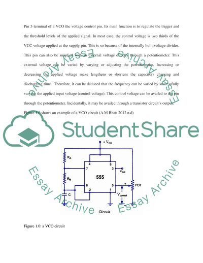
StudentShare
Contact Us
Sign In / Sign Up for FREE
Search
Go to advanced search...
Free

Designing and Testing of a Delay Unit - Lab Report Example

Cite this document
Summary
The paper "Designing and Testing of a Delay Unit" describes that the voltage controlled oscillator was developed and tested by doing various procedures in the experiment. The properties of how different parameters change relative to others were observed in designing the VCO…
Download full paper File format: .doc, available for editing
GRAB THE BEST PAPER95.6% of users find it useful
Designing and Testing of a Delay Unit
Read Text Preview

Extract of sample "Designing and Testing of a Delay Unit"

Design, implement, and test a timer (Prototype Product) EXPERIMENT REPORT SUBMISSION PART 4: EXPERIMENT: DESIGNING AND TESTING OF A DELAY UNIT OBJECTIVES: To explore the property of 555 chip through experiments To design and test a Voltage Controlled Oscillator (VCO) To build a 555-based delay unit To design and build a trigger circuit To strengthen your practical skills THEORY OF THE EXPERIMENT: Voltage Controlled Oscillator can be defined as a module that generates the frequency of the notes audible by human ears.  This allows the user to accurately "tune and set" the pitch source.  A VCO can be compared to a single string from a guitar.  When the guitar string is plucked, it generates a specific note. A VCO has a 1V/OCT CV input.  The CV originates mainly from the keyboard controller.  This CV changes the pitch of the VCO just the same way a guitar string changes the guitar. The VCO circuit can also be called a voltage-to-frequency converter. This is because its output frequency can be varied by varying the input voltage. Pin 5 terminal of a VCO the voltage control pin. Its main function is to regulate the trigger and the threshold levels of the applied signal. In most case, the control voltage is two thirds of the VCC voltage applied at the supply pin. This is so because of the internally built voltage divider. This pin can also be supplied with an external voltage directly through a potentiometer. This external voltage can be varied by varying or adjusting the potentiometer. Increasing or decreasing the applied voltage make lengthens or shortens the capacitors charging and discharging time. Therefore, it can be deduced that the frequency can be varied by successfully varying the applied input voltage (control voltage). This control voltage can be availed to the pin through the potentiometer. Incidentally, it may be availed through a transistor circuit’s output. Figure 1.0 shows an example of a VCO circuit (A.M Bhatt 2012 n.d) Figure 1.0: a VCO circuit Voltage-controlled oscillator uses the 555 timer IC as the core component this IC should be configured first to form an astable multivibrator before it is used as an oscillator. An astable multivibrator can be defined as a timing circuit with an output that oscillates between the logics low and high without stopping, as a result, it creates a full train of pulses. The main difference between this circuit and the standard 555 timer circuit is that the 555s pin 5 is connected to an external voltage supply.  Pin five is the 555s control voltage pin. This pin allows the user to adjust the threshold voltage. This is the voltage that pin two and pin six are compared to by the internally built comparators. The outputs from these comparators normally controls the internally built flip flop circuits that toggles 555 timer’s output, then, adjusting the control voltage at pin five varies the frequency at which the 555 timer’s output is toggled at. Increased voltage at pin 5 decreases the output oscillation frequency. Decreasing this voltage increase the oscillation frequency at the output.         EQUIPMENTS AND COMPONENTS USED: Equipment: Breadboard, DC Power Supply Unit (PSU), Digital Multi-Meter (DMM), Oscilloscope Components: Resistors (Ω): 330kΩ, 200k, 5×100k, 2×5.1k, 1k, 82, Capacitors (F): 10n, 22n 100μ (Tantalum), Chips: LMC555CN), LEDs: LED, Switch: On/Off Switch Figure 1.1: a 555 timer based VRO EXPERIMENTAL PROCEDURE 555-based oscillator was designed and built on a breadboard as shown figure 1.3 Figure 1.3: A VRO circuit Maximum and minimum values of V2 and Vout, and the durations were recorded. RA was increased to 330 kΩ and observations recorded. RA was reset to 100 kΩ and RB changed to 330kΩ and test 1 was repeated RA was set to be equal to RB=100kΩ and the supply voltage was reduced to 6V and test 1 repeated. The supply voltage was reduced to 3V and the test 1 was repeated Vcc was set to 9V and a voltage of 5V was applied to pin 5. Then V5 was changed between 0 and 8 V in steps of 1V. The minimum and maximum values of V2 and Vout together with the frequency were recorded. A graph of V2 (Maximum), V2 (Minimum), Vout (Maximum), and frequency against V5 was plotted RESULTS AND DISCUSSION DISCUSSION QUESTIONS Comparing the waveform of Vout with the waveform of Vc for the NOR gate based oscillator. It can be observed that the waveform for the 555 timer oscillator is square wave while for the NOR gate based oscillator was a triangular wave. It can also be observed that when the value of RA was increased, the amplitudes of the waves increase proportionally with respect to the increase in the value of resistance. Also the output voltage value increases proportionally from 2.8 V to 10 V. Setting RA to 100 kΩ and RB to 330kΩ. Then the duration for Vout=’high’ decreases from 2.98ms to 1.386ms while the Vout=’low’ duration remains constant. When RA was set to be equal to RB=100kΩ and the supply voltage was reduced to 6V, then the Maximum voltage= 7 V, minimum voltage= -200mV Based on the tests 3 and 4, then the relationship between the following values is as follows: The maximum value of V2 – Vcc is inversely proportional to V2 The minimum value of V2 - Vcc is directly proportional to V2 The maximum value of Vout - Vcc is directly proportional to Vout. GRAPHS Why frequency changes? This is because the voltage change also changes the impedance for the circuit which means the capacitance is changed. Frequency is inversely proportional to the capacitance. And is related by the equation= 1/ (1.386R2*C) PART 5: PUTTING TOGETHER AND CALIBRATION OBJECTIVES: To interface the delay unit, oscillators and amplifier To calibrate the system To strengthen practical skills Theory of experiment Oscillators An oscillator can be defined as an oscillator circuit that generates oscillating electronic signal, periodic signal or at times square waveforms or sine waveforms. They convert direct current from the source to AC signals (alternating current) any electronic devices are used for this purpose. Some conspicuous examples of signals produced by oscillators include broadcasted signals from radios and televisions, computer’s clock signals and crystal quartz clock circuits. Sounds produced by electronic beepers and from video games are also examples these signals. COMPONENTS AND EQUIPMENT Equipment: Breadboard, DC Power Supply Unit (PSU), Battery: 9V with connectors, Digital Multi-Meter (DMM), Oscilloscope, Screwdriver Components: Resistors (O): 10k, 300k, 5×620k, Capacitors (F): 33µ, Potentiometer (O): 50k Linear Carbon, Multi-position switch Note: All resistors are of 0.25W Metal Film (: 1%) EXPERIMENTAL PROCEDURE 1. Interfacing The delay unit was connected to the oscillator as shown in the figure 2. Calibration a. The potentiometer was connected as shown in the figure b. For R3=620kΩ, the delay was adjusted to 60 sec 3. The circuit given in fig. 5.3 was built using a multi-position switch, and testing for the delay was done and recorded for each value of R3. 4. The power supply was replaced with a 9V battery, observations made. RESULTS AND DISCUSSION Delay(min) 0.5 1 2 3 4 5 R3(k) 310 620 1240 1860 2480 3100 Discussion questions Q1: To disable the above NOR gate, should the ‘control signal’ be ‘high’ or ‘low’? (Hint: Use the logical properties of NOR gates) Answer: the control signal should be high for disabling Q2: What is the output of the delay unit (pin 3 of 555) before the required delay is reached? Answer: Vout=9 V 4. Q1: What is the function of C5? 5. Answer: this capacitor is used to make sure that the system does not lose power since it will be charging and discharging at intervals 6. Q2: Why do we use two switches (S1 and S2)? 7. Answer: S2 is a safety switch in that it protects the components in case of any malfunction. S1 is the systems switch for switching on and off based on status of the capacitor. CONCLUSION The voltage controlled oscillator was developed and tested by doing various procedures in the experiment. The properties of how different parameters change relative to others were observed in designing the VCO, and this has strengthened our practical skills on 555 timer based oscillators. Also comparison showed that the waveform for 555 timer based oscillator is rectangular in shape while that of a NOR gate-based oscillator is a triangular wave. References Professor Barry Parton 1998, Fundamentals of Digital Electronics, National Instrument Corporation John Bird 2007, Electrical and Electronics Principals and Technology, third edition Newnes Elsivier UK Collin Mitchell 2012, 50-555 timer circuits, Talking Electronics Anil K. Maini 2007, Digital Electronics, Principle, Devices and Application, John Wiley and Son Limited, England Read More
Tags
Cite this document
  • APA
  • MLA
  • CHICAGO
(Design, implement, and test a timer (Prototype Product) ( electrical ) Lab Report Example | Topics and Well Written Essays - 1750 words, n.d.)
Design, implement, and test a timer (Prototype Product) ( electrical ) Lab Report Example | Topics and Well Written Essays - 1750 words. https://studentshare.org/engineering-and-construction/1872950-design-implement-and-test-a-timer-prototype-product-electrical
(Design, Implement, and Test a Timer (Prototype Product) ( Electrical ) Lab Report Example | Topics and Well Written Essays - 1750 Words)
Design, Implement, and Test a Timer (Prototype Product) ( Electrical ) Lab Report Example | Topics and Well Written Essays - 1750 Words. https://studentshare.org/engineering-and-construction/1872950-design-implement-and-test-a-timer-prototype-product-electrical.
“Design, Implement, and Test a Timer (Prototype Product) ( Electrical ) Lab Report Example | Topics and Well Written Essays - 1750 Words”. https://studentshare.org/engineering-and-construction/1872950-design-implement-and-test-a-timer-prototype-product-electrical.
  • Cited: 0 times

CHECK THESE SAMPLES OF Designing and Testing of a Delay Unit

Speech to an existing presentation etc. - Control System Design Knowledge requested

This will cause a delay of several days that we did not expect.... The system comprises of three parts; flight monitoring unit, which is our own unit, safety unit together with radar and defense system.... The flight-monitoring unit is divided into four partners but since we are the system OEM we are responsible for the completely functioning processes of the unit.... Bankarottair does software integration after Rashid air has completed the software acceptance testing....
5 Pages (1250 words) Term Paper

New Tablet PC Project: HP TouchPad2

This paper details the project management considerations for the development of the HP TouchPad2, the second generation of HP tablets featuring several improvements.... Herein, details about the external and internal project determinants are provided alongside a PERT and Gantt chart for the project....
7 Pages (1750 words) Assignment

PRINCE2 (Project IN Controlled Environment)

It is pertinent to mention here that the term ‘product' can be an intermediate document, requirement specification document, user accepting testing documentation and so on.... PRINCE2 (Project IN Controlled Environment) is a project management standard used in more than 150 countries for successfully managing a project....
5 Pages (1250 words) Essay

Balance Sheet and Cost Reduction of Sidcup Furnishings

nbsp;  The cost of direct materials has increased over the years meaning that this could have caused an increase in the cost of production for a unit.... The author analyzes the information contained in the extracts from the profit and loss for Sidcup Furnishings.... The author also indicates the possible areas of weaknesses in the material, labor, and overhead costing and control practices and procedures in the factory of the company....
7 Pages (1750 words) Coursework

Why did it take Africa 32 years of negotiation to sign the Treaty of Pelindaba

This declaration came about in response to the United Nation's call for unity against the testing of nuclear weapons in Africa; this declaration was triggered by the events that followed the nuclear testing of France in the Sahara Desert (Academie de Droit International de la Haye, p....
3 Pages (750 words) Essay

Young at Heart Centre

The purpose of this project plan is to present a detailed project management plan of preparation of an annual report of the Young at Heart Centre performance results, accomplishments and financial status The main assumption of this project is that more interactive, colorful and… user-friendly version of the Yong At Heart annual report will enable the Centre to get to “in the same league” with other large not-for-profit organizations with which it feels it competes for donations and funds....
8 Pages (2000 words) Essay

Parphrase for ibrahim

Its purpose is the detection of the third within the railing in the voltage and this is supposed to be High on voltage intensity.... For the Output Pin to extract a High state output, the Pin number 2 has to go into Low state along with the… A contrast in the form of Higher state at Pin number 6 and Lower state at Pin number 2 will yield a Low Volate output....
6 Pages (1500 words) Essay

Operations Strategy and Timeline of Managed Project

The current length of the critical path will increase by three weeks as due to the delay of three weeks in activity H.... The three weeks delay in activity H can be handled appropriately by shortening the times that the next activities consume.... he activity H lies on the critical path and the delay in this activity will cause serious troubles regarding the extension in critical time for the completion of the project.... The time taken on the critical path will be:The activity H is the user acceptance testing which is a critical activity in this project as the activity lies on the critical path....
5 Pages (1250 words) Coursework
sponsored ads
We use cookies to create the best experience for you. Keep on browsing if you are OK with that, or find out how to manage cookies.
Contact Us