StudentShare

Our website is a unique platform where students can share their papers in a matter of giving an example of the work to be done. If you find papers
matching your topic, you may use them only as an example of work. This is 100% legal. You may not submit downloaded papers as your own, that is cheating. Also you
should remember, that this work was alredy submitted once by a student who originally wrote it.
✕
Free
Electronic Systems - Lab Report Example
Summary
This lab report "Electronic Systems" aims at building and gaining offset circuit through two steps: collect the preset and recommended amplifiers and make a connection between the two amplifiers being tested. …
- Subject: Engineering and Construction
- Type: Lab Report
- Level: Undergraduate
- Pages: 5 (1250 words)
- Downloads: 0
- Author: schroederhilma
Extract of sample "Electronic Systems"
Electronic Systems Lab Gain and Offset Circuit Introduction A build and gain offset circuit can be set up through two steps as follows
Collect the preset and recommended (required) amplifiers
Make a connection between the two amplifiers being tested
Equipment
The equipment that is to be used in the experiment includes:
A Digiac 3000 operational amplifiers
Signal generator
Twin beam oscilloscope with probes
Procedure
Connect the circuit as shown:
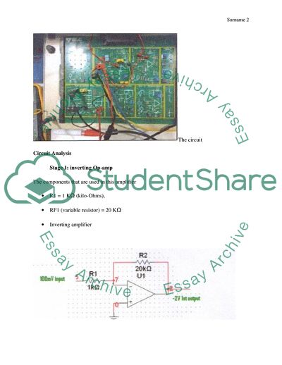
The circuit
Circuit Analysis
Stage 1: inverting Op-amp
The components that are used in this amplifier
R1 = 1 KΩ (kilo-Ohms),
RF1 (variable resistor) = 20 KΩ
Inverting amplifier
Inverting amplifier used to convert and amplify input signal
Vout = Vin
Vout = X 100 X 10-3 = -2 Vp-p
Gain = = = -20
Stage 2: summing Op-amp
Components used in this set up include
R2 – 75 KΩ
R3 = 75 KΩ
RF2 = 75 KΩ
Summing amplifier
V1 offset = -2.5 V (DC)
The inputs to the summing up amplifier are:
V1 = -2.5 V
V2 = -2Vp-p (AC)
Summing up the amplifier converts the input AC and DC Offset voltage.
By cancelling out the resistors of equal value, then:
Gain 2 = = = -1
The total outcome of the amplification
Gain 1 = -20
Gain 2 = -1
The total gain = G1*G2 = -20 X -1 = 20
Required for Mode A
Measure the bandwidth of your amplifier, by locating the upper 3 dB point. Can you relate this to published data of the op amps used?
Band width = 70.8 x 10 3 – 100 = 70.7 KHz
Conclusion
The experiment was of great use. I ensured that the gain and offset circuit used for calibration were the actual values used for the amplification. I observed that the input signal was in phase with the final output signal, which was derived from summing the Op amplifiers. The input signal used was a 100 mV adjusted from the signal generator by changing the amplitude of S.G. as having chosen the 1 K and 20 KΩ resistors to get the value 20 after summing up the amplifiers with the second op Amp being used to control the audio frequency (Bird 291).
Lab 2: Filter Circuits 1
1. The response of a High Pass Filter is represented by:
2. The response of a Band Pass Filter is represented by:
3. A suitable schematic of a simple RC low pass filter is represented by:
4. A suitable schematic of a simple RC high pass filter is represented by:
5. A simple RC high pass filter has a resistor of 6.8 KΩ and a capacitor of 4.7 nF. The cut off frequency will be:
c. 5 KHz
6. A simple RC low pass filter has a resistor R of 2.2 KΩ and a capacitor of 3.9 nF. The cut off frequency will be:
a. 18.5 KHz
Lab 3:
In modern electronic systems its common to find both digital and analogue circuits with conversion of data happening based on the conditions of the circuit, i.e. Digital to analogue and vice versa. This experiment is designed to explore simple design principles of the digital to analogue Converter (DAC) via use of the R–2R ladder.
Procedure
A 2.5 voltage reference is used and the output is approximated at 7.5 on connecting a zener diode to the 10 KΩ resistor that provides 2.5 volts from the 12 V main power source.
The DAC is tested by first connecting its digital input to the CK342A board switches and the following data is collected.
Input switches
Analogue output voltage
S3
S2
S1
S0
0
0
0
0
0.0V
0
0
0
1
-0.46V
0
0
1
0
-0.93V
0
0
1
0
-1.39V
0
1
0
0
-1.86V
0
1
0
1
-2.33V
0
1
1
0
-2.80V
0
1
1
1
-3.27V
1
0
0
0
-3.76V
1
0
0
1
-4.23V
1
0
1
0
-4.70V
1
0
1
1
-5.17V
1
1
0
0
-5.64V
1
1
0
1
-6.11V
1
1
1
0
-6.57V
1
1
1
1
-7.04V
To measure the output value by solving the equation:
Output = X Vref
Such as the binary code 1011, the output is given by
= X 17 = -6.093 V, and so on for all binary numbers
The output shall fall within the rage of 0.46 V to 7.04 V
Measure the current flowing into the R-2R ladder.
The current flowing into the R-2R ladder is 0.25 mA
Now connect the DAC inputs to the outputs of the 7HC193 counter on the CK34A, ensuring MSB is connected to MSB etc. Drive the counter from the on-board clock, labeled CK out. Select a suitable clock frequency. Observe the DAC output on the Oscilloscope.
Measure the clock frequency and record in as much detail as possible (including photograph or sketch) the output of the DAC.
The output frequency from the DAC can be obtained from the calculation:
T = 6.8 x 0.2 = 735 Hz.
The reading from the clock shows that the highest voltage recorded from the digital signal is 7.04 V and the lowest being 0.47 V conforming to the stated statement from the binary form calculations.
Conclusion
The digital to analogue converter aids in identifying digital inputs through an analogue and image technique. This experiment is an exhibition of how a digital signal is converted into an analogue output, which is helpful in solving and designing digital circuits in practice.
Works Cited
Bird, J. Electrical and Electronic Principles and Technology. 2nd ed. Burlington: Newnes, 2003. Print.
Read
More
sponsored ads
Save Your Time for More Important Things
Let us write or edit the lab report on your topic
"Electronic Systems"
with a personal 20% discount.
GRAB THE BEST PAPER
