StudentShare
Contact Us
Sign In / Sign Up for FREE
Search
Go to advanced search...
Free

Metal-Insulator-Semiconductor Contacts, and Spin Coating - Assignment Example

Cite this document
Summary
The paper "Metal-Insulator-Semiconductor Contacts, and Spin Coating" highlights that the atomic force microscope was developed by Binnig, Quate and Gerber in 1985 in order to enable the study of materials by doing non-destructive surface profilometry at a very high resolution…
Download full paper File format: .doc, available for editing
GRAB THE BEST PAPER92% of users find it useful
Metal-Insulator-Semiconductor Contacts, and Spin Coating
Read Text Preview

Extract of sample "Metal-Insulator-Semiconductor Contacts, and Spin Coating"

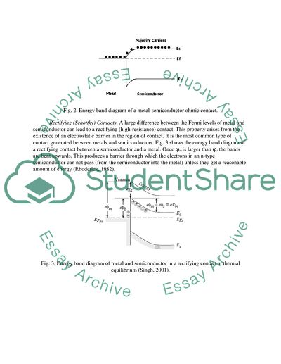
Metal-Semiconductor Contacts The metal- semiconductor contact was the first practical semiconductor device. When there is a contact between a metal and a semiconductor, their Fermi levels must be equal at equilibrium (Sze, 2006). The work function of the metal (q.φm) is usually different from the work function of the semiconductor (q.φs) and a barrier is formed at the metal-semiconductor interface. Work function is the energy the electron must be provided with in order to move from the Fermi level into vacuum. The choice of materials (metal and semiconductor) can result in different types of contacts: (1) nonrectifying or ohmic contact and (2) rectifying or Schottky contact. The barrier presents and capacitance behavior and the flux of carrier from one material to another will be controlled by it. Fig. 1 shows the energy band diagram of a metal and a semiconductor isolated from each other. Fig. 1. Energy band diagram of disconnected metal and n-type semiconductor (Singh, 2001). EV is the energy level in the valence band, EC is the energy level in the conduction band, EF is the Fermi level, χs is the electron affinity for the semiconductor, e (or q) is the carrier charge, φB is the Schottky barrier height. Vbi is the built-in potential. This potential is seen by electrons in the conductor band of the semiconductor when they try to move into the metal. Ohmic Contacts. An ohmic contact is a low resistance contact that is formed when the Schottky barrier height q.φB is zero or negative. The barrier height is the difference between the metal work function and the semiconductor electron affinity: For an n-type semiconductor it means that the work function of the metal is similar or lower than the difference between the energy at vacuum level and the lower energy level of the conduction band and the energy bands are bent downwards (Rhoderick, 1982). Fig. 2 shows the energy band diagram of an ohmic contact. An ohmic contact between a p-type semiconductor and a metal takes place when the work function of the metal is larger than the sum of the electron affinity and the bandgap energy. In this case the carriers (holes) need a low energy to pass through the contact. Fig. 2. Energy band diagram of a metal-semiconductor ohmic contact. Rectifying (Schottky) Contacts. A large difference between the Fermi levels of metal and semiconductor can lead to a rectifying (high-resistance) contact. This property arises from the existence of an electrostatic barrier in the region of contact. It is the most common type of contact generated between metals and semiconductors. Fig. 3 shows the energy band diagram of a rectifying contact between a semiconductor and a metal. Once φm is larger than φs the bands are bent upwards. This produces a barrier through which the electrons in an n-type semiconductor can not pass (from the semiconductor into the metal) unless they get a reasonable amount of energy (Rhoderick, 1982). Fig. 3. Energy band diagram of metal and semiconductor in a rectifying contact at thermal equilibrium (Singh, 2001). Metal-Insulator-Semiconductor Contacts The metal-insulator-semiconductor (MIS) structure was first proposed as a voltage-controlled capacitor in 1959 (Sze, 2006). The ideal MIS capacitor has an insulator with infinit resistivity. The only charges it presents are those in the semiconductor and those on the metal surface close to the insulator, under any biasing conditions. Fig. 4 shows the structure where V is the applied voltage and d is the thickness of the insulator. Fig. 4. Structure of a metal-insulator-semiconductor (MIS) capacitor (Sze, 2006). The energy band diagram of a metal-insulator-semiconductor structure without bias is shown in Fig. 5. The band is flat when no voltage is applied. Fig. 5. Energy-band diagrams of ideal MIS capacitors without bias. (a) n-type semiconductor. (b) p-type semiconductor (Sze, 2006). EV is the energy level in the valence band, EC is the energy level in the conduction band, Eg is the band gap, EF is the Fermi level, Ei is the intrinsic Fermi level, φm is the metal work function, χ and χi are the electron affinities for the semiconductor and the insulator respectively, and ψB is the potential difference between EF and Ei (Fey Lin, 1988). Fig. 6 shows what happens to the energy-band at the semiconductor surface when a positive or a negative voltage is applied to the structure. When the metal plate is biased with a negative voltage, as in Fig. 6(a), the valence-band edge EV bends upward near the surface and is closer to the Fermi level, which remains flat in the semiconductor. This is the accumulation mode, since it causes an accumulation of majority carriers (holes) near the semiconductor surface. When the metal plate is biased with a slightly positive voltage, the bands bend downward, and the carriers are depleted, as in Fig. 6(b). When the voltage is more positively increased, the bands bend even more until the number of minority carriers (electrons) is larger than the majority carriers, causing an inversion on the surface, as in Fig. 6(c). Fig. 6. Energy-band diagrams of ideal MIS capacitors with bias for a p-type semiconductor (Sze, 2006). Basic Principles of Transistors The word transistor is actually a contraction of transfer resistor. The bipolar transistor is a very important semiconductor device, but the most used device for advanced integrated circuits is the metal-oxide-semiconductor field-effect transistor (MOSFET). The bipolar transistor can perform conduction with both types of carriers, electrons and holes, while the field-effect transistors, like MOSFET, perform conduction with predominantly one type of carrier (Sze, 2006). The MOSFET is a four terminal device that can operate in three different regions – cut-off, linear and saturation regions – that states the current it can supply depending on the voltages applied to those terminals (RABAEY, 2005). The voltage applied to the gate terminal determines the amount of charge available in the channel between the source and the drain ports, and consequently the path resistance. The potential difference between these terminals determines the amount of current that flows through the channel. Ideally, there is no current flowing between the gate terminal and the channel, since the input impedance of the transistor is very high. According to the structure, the MOSFET has two types of devices. The NMOS transistor consists of n+ drain and source regions, embedded in a p-type substrate. The current is carried by electrons in an n-type channel. PMOS transistors are made by using an n-type sustrate and p+ drain and source regions. The current is carried by holes moving in a p-type channel. Mobility The carriers in the semiconductor are in constant motion due to thermal energy. This random motion results in no net displacement over a certain period of time. This is caused because the carriers collides with lattice atoms and impurities, what results in random scattering. When an electric field is applied to the semiconductor, the electrons will not be moving randomly, but rather in a preferential direction. The mobility of the carriers is a measure on how the applied electric field influences the motion of the carriers. Threshold Voltage The conducting channel between drain and source is only formed when a certain voltage is applied to the gate terminal. The minimum voltage at the gate terminal that is able to create the channel is called the threshold voltage (VTH). Current is then allowed to flow through the channel is a difference of potential is applied between the gate and source ports. Regions of Operation a) Cut-off Region For zero potential between gate and source (VGS = 0) and the ground potential connected to drain, source and substrate, there is no charge density in the region between drain and source, resulting in a high resistance channel. Under these conditions, the transistor is cut-off, since almost zero current flows from drain to source. b) Linear (Resistive) Region In the case of a NMOS, a positive difference of potential applied between gate and source (VGS > 0) leads to an accumulation of negative charge on the substrate side. For VGS larger than VTH, the charges so placed form an inversion layer at the semiconductor surface and a depletion layer below the gate. Fig. 7: NMOS transistor operating in the linear region (Rabaey, 2005). If a potential difference is applied between drain and source terminals, a current will flow along the channel. The channel is capacitively controlled by the electric field that is formed by the voltages applied to the terminals. The larger the voltage difference between gate and source, the smaller the resistance of the conducting channel and the larger the current (Srivastava, 2005). If the drain potential is relatively small, the transistor operates in the linear (also called resistive or triode) region because the channel acts as a resistor. The drain current ID - a current flowing from drain to source - is proportional to the drain voltage. c) Saturation Region When the drain-source potential (VDS) increases and reaches a saturation value (VDSAT = VGS – VTH), the thickness of the inversion layer is reduced to zero at some point (pinch-off point) close to the drain region. Beyond the value of VDSAT the drain current remains essentially the same and it characterizes the saturation region (Fig. 8). Fig. 8: NMOS transistor under pinch off conditions (Rabaey, 2005). As a coarse approach, the transistor can be conceived as a switch. The switch is closed (“on”) when the device is conducting and open (“off”) when there is no current flowing through the device. Organic Thin Film Transistors Organic semiconductors can be classified in small molecules and polymers. Small molecules have a well-defined structure while polymers consist of organic chains and they may grow in an amorphous way (De Vusser, 2006). A very important organic semiconductor is the pentace, an oligocene with five repeating units. Fig. 9 shows the structure of some organic semiconductors. Fig. 9. Chemical structure of some organic semiconductors (Coropceanu, 2007). Research on organic-based electronic devices has been extensively performed during the last years. The use of organic semiconductors has been encouraged because of some advantages they have when compared to the well-known Si technology (De Vusser, 2006): (1) the process of organic semiconductors can be carried on at low temperatures, (2) the absence of dangling bonds in organic molecules makes it possible to deposite the thin films on different types of substrates, and (3) the possibility of synthesizing a large variety of organic semiconductors provides the ability of adjusting some of their properties in order to meet the requirements of certain applications. Fig. 10 shows two different structures of organic thin film transistors (OTFT). Fig. 10. OTFT device configurations: (a) top-contact device and (b) bottom-contact device (Dimitrakopoulos, 2002). The charge transport in semiconductors is very dependent on the structure and morphology. The conductivity in a organic semiconductor formed by small molecules is determined by the inter-molecular transport, since an organic material is composed of weakly bonded molecules. Fig. 11 shows a three-dimensional structure of a thin film transistor with the applied voltages. Fig. 11. The 3D structure of a thin film transistor (Zhu, 2003). Fabrication and Characterization of Pentacene Thin Film Transistors The use of organic thin films of small molecules, like pentacene (C22H14), has been widely researched. Besides, pentacene-based transistors can be easily interfaced with the current Si technology. The growth of pentacene results in polycrystalline films with a relatively high charge carrier mobility and can be performed on various low cost substrates (Lin, 1998). The pentacene thin film mobility is ≥ 1 cm2 / V.s. Fig. 12 shows the Lewis structure of a pentacene. Fig. 12. Lewis structure of a pentacene (Schiefer, 2007). Fabrication of pentacene thin films on large areas has two promising methods: organic phase deposition and thermal evaporation. (Knipp, 2004) used a thermal evaporation system to deposit the pentacene films to process the transistor with bottom-gate configuration presented in Fig. 13. Glass was used as substrate and an inorganic dielectric was processed upon it. The pentacene was then deposited on the top of the dielectric. Fig. 13. Pentacene TFT on a glass substrate (Knipp, 2004). Physical vapor deposition (PVD) is one of the techniques that can be used to deposit small organic molecules, but the most common technique used is organic molecular beam deposition (OMBD) (Janssen, 2006), though it has the disadvantage of requiring (ultra)high vacuum. In this process, an organic material in a vacuum chamber has its temperature increased and a beam of evaporated molecules is ejected onto a substrate. Crystal nuclei are then formed by these molecules on the surface and a polycrystalline thin film is typicall resulted as more molecules are deposited. The thin film morphology is strongly influenced by the substrate temperature and deposition rate. Another technique, organic vapor phase deposition (OVPD), uses a gas carrying organic semiconductor molecules at low vacuum to deposit the thin film onto a substrate. The I-V characteristics of a top-contact pentacene OTFT are presented in Fig. 14. It is a plot of the drain current ID versus the drain voltage VD of the transistor for different gate voltages VG. Fig. 14. I-V characteristics of a pentacene OTFT (Dimitrakopoulos, 2002). Pentacene thin film transistors are p-type semiconductors (holes are the majority carriers). When a negative voltage is applied to the gate terminal the device operates in the accumulation mode. It means that the channel has a large concentration of carriers accumulated, what results in a low resistance path and current can flow through it (Dimitrakopoulos, 2002). Spin Coating The spin coating technique was first used in the fabrication of thin, uniform films of paint, varnish and asphalt (Washo, 1977). It is a technique used for application of thin films to surfaces. In modern semiconductor manufacturing, spin coating is a very-well known process to deposit photoresist on wafers. The aggressive shrinking of semiconductor devices demands more uniform photoresit films. This is very important for the lithography step of the process fabrication. Spin coating can produce organic thin films with thicknesses ranging from nanometers to micrometers. The spin coating process can be divided in four major steps: (1) the deposition (the solid coating material is dissolved in a solvent and placed on the substrate), (2) the spin up, (3) the spin off and (4) the evaporation (Luurtsema, 1997). The principle of spin coating is shown in Fig. 15. Fig. 15. Spin coating stages (Luurtsema, 1997). Deposition Stage This first stage, also called the dispense stage, involves the application of an excessive amount of coating solution onto a substrate that is put to spin. The fluid must wet the surface completely otherwise incomplete coverage can result. The amount of solution dispensed is larger than the amount that is required in the final coating thickness. Spin up Stage In this second stage the substrate is accelerated until it reaches the final spin speed. In this step of the process there is usually some amount of fluid expulsion from the wafer surface by the rotational motion. It may happen that the film formed at this step by the fluid is thin enough and will be rotating along with the wafer, what eliminates thickness differences. Spin off Stage Centripetal acceleration resultant from the high-speed spinning substrate will cause the material to spread, producing a uniform coating while the solvent evaporates (Faller, 2009). This stage is characterized by gradual fluid thinning what happens primarily by centrifugal forces until a reasonable amount of solvent has been eliminated. Then the behavior of the flow is dominated by the fluid viscous forces. Evaporation Stage In this stage the substrate is rotating at a constant rate and the coating thinning is dominated by the solvent evaporation. Though evaporation takes place throughout the spin coating process, it is very important at this point. This is a critical step in defining the final film thickness. The final film thickness will strongly depend on the properties of the coating material, such as viscosity, drying rate, surface tension, and on the parameters of the spin process, mainly the speed. Atomic Force Microscopy The atomic force microscope was developed by Binnig, Quate and Gerber in 1985 (Binnig, 1986) in order to enable the study of materials by doing non-destructive surface profilometry at a very high resolution. Atomic Force Microscopy (AFM) is a technique used to obtain three-dimensional (axes x, y and z, normal do the sample surface) images of a sample surface. AFM has been used to analyze van der Waals forces, repulsive forces, lateral friction forces and magnetic forces (Albrecht, 1988). It is able to map the contours of the surface of conducting and insulating materials. The technique requires neither any special sample preparation nor a vacuum environment. The images are obtained by scanning a sharp probe across the surface while the interactions of the tip and the sample are analyzed (Blanchard, 1996). The spatial dependence of the interaction force between the tip and the sample is characterized by scanning the sample across the tip, while the distance between them is adjusted to keep the deflection of the cantilever constant. The detection system is able to verify extremely small deflections of the cantilever, so very small interaction forces can be measured. AFM can be classified as repulsive (contact) or attractive (noncontact) mode, according to the interation of the tip and the sample surface. In the attractive force mode the tip does not touch the sample, but stays quite close to it. The tip is vibrated and a detection system with a laser measures the vibration and provides an electrical signal according to it (Martin, 1994). The vibrations are closely related to the distance between the tip and the sample, so the electrical signal generated is also related to the tip-sample spacing. The resonant frequency or amplitude of the oscillating cantilever is the aimed measurement. Fig. 16 shows the principle of AFM in contact mode. The technique relies on forces between the tip and the sample which are related to the deflections of the lever as it scans the sample. In order to measure these displacements a laser shines on the tip and eventual changes in the reflected beam are able to provide image resolution on the atomic level (under ideal conditions). Fig. 16. The principle of AFM (Kucera, 2010). Fig. 17 shows an image generated by a contact mode AFM in order to reveal the atomic structure of mica. Fig. 17. Image of the surface of mica generated by a contact mode AFM (Blanchard, 1996). Works Cited Albrecht, T. R., Quate, C. F. Atomic Resolution with the Atomic Force Microscope on Conductors an Nonconductors. Journal of Vacuum Science and Technology A 6.2 (1988): 271-274. Binnig, G., Quate, C. F., Gerber, C. Atomic Force Microscope. Phys. Rev. Letter 56.9 (1986): 930-933. Blanchard, Cheryl R. Atomic Force Microscopy. The Chemical Educator 1.5 (1996). Coropceanu, V. et al. Charge Transport in Organic Semiconductors. Chem. Rev. 107.4 (2007):926-952. De Vusser, Stijn. Organic Thin-Film Transistors: Process Technology and Circuit Design. Thesis. Katholieke Universiteit Leuven, 2006. Dimitrakopoulos, C. D., Malenfant, P. R. L. Organic Thin-Film Transistors for Large Area Electronics. Adv. Mater 14.2 (2002): 99-117. Faller, Roland et al. Biomembrane Frontiers: Nanostructures, Models, and the Design of Life. Humana Press, 2009. Fey Lin, B. S. Electrical Studies of Metal-Insulator-Semiconductor Structure. Thesis. Texas Tech University, 1988. Knipp, D., Street, R. A. Pentacene Thin Film Transistors on Large Area Compatible Gate Dielectrics. Journal of Non-Crystalline Solids (2004):595-598. Kucera, O. Electrical Analogy to an Atomic Force Microscope. Radioengineering 19.1 (2010):168-171. Janssen, Dimitri. Self-Assembling Monolayers for Organic Thin-Film Transistors. Thesis. Katholieke Universiteit Leuven, 2006. Lin, Y. Y., et al. Stacked Pentacene Layer Organic Thin-Film Transistors with Improved Characteristics. IEEE Electron Device Letters 18 (1997): 606-608. Luurtsema, G. A. Spin Coating for Rectangular Substrates. Thesis. University of California, 1997. Martin, Y., Wickramasinghe, K. Method for Imaging Sidewalls by Atomic Force Microscopy. Applied Physics Letters 64.19 (1994): 2498-2500. Rabaey, J.M.; Chandrakasan. A.; Nikolic, B. Digital Integrated Circuits: A Design Perspective. 2nd ed. Upper Saddle River: Prentice Hall, 2005. Rhoderick, E. H. Metal Semiconductor Contacts. IEE Proc. 129.1 (1982): 1-14. Schiefer, S. Crystal Structure of Fiber Structured Pentacene Thin Films. Dissertation. Ludwig-Maximilians-Universität, 2007. Singh, J. Semiconductor Devices: Basic Principles. John-Wiley, 2001. Srivastava, A., Sylvester, D., Blaauw, D. Statistical Analysis and Optimization for VLSI: Timing and Power. New York, NY, USA: Springer, 2005. Sze, S. M., Kg, K. K. Physics of Semiconductor Devices. New Jersey: John Wiley & Sons, Inc, 2006. Washo, B. D. Rheology and Modeling of the Spin Coating Process. IBM Journal of Research and Development. 21.2 (1977): 190-198. Zhu, Wen Wei. Organic Thin Film Transistor. Thesis. McGill University, 2003. Read More
Cite this document
  • APA
  • MLA
  • CHICAGO
(Fabrication, and Characterization of Pentacene Thin Film Transistor, Assignment, n.d.)
Fabrication, and Characterization of Pentacene Thin Film Transistor, Assignment. Retrieved from https://studentshare.org/technology/1740865-background-metal-insulator-semiconductor-contacts-spin-coating-fabrication-and-characterisation-of-pentacene-thin-film-transistor-different-organic-thin-film-transistor-structuresafm-atomic-force-microscopy
(Fabrication, and Characterization of Pentacene Thin Film Transistor, Assignment)
Fabrication, and Characterization of Pentacene Thin Film Transistor, Assignment. https://studentshare.org/technology/1740865-background-metal-insulator-semiconductor-contacts-spin-coating-fabrication-and-characterisation-of-pentacene-thin-film-transistor-different-organic-thin-film-transistor-structuresafm-atomic-force-microscopy.
“Fabrication, and Characterization of Pentacene Thin Film Transistor, Assignment”, n.d. https://studentshare.org/technology/1740865-background-metal-insulator-semiconductor-contacts-spin-coating-fabrication-and-characterisation-of-pentacene-thin-film-transistor-different-organic-thin-film-transistor-structuresafm-atomic-force-microscopy.
  • Cited: 0 times

CHECK THESE SAMPLES OF Metal-Insulator-Semiconductor Contacts, and Spin Coating

Development of Pad Conditioner Drop Detection System

spin etch planarization (SEP) 10 2.... spin on deposition (SOD) 11 SOP is mostly applied in deposits on different glasses, porous low-k dielectrics and polymer ILD.... Nevertheless, several defects are noted on the spin in the deposited materials.... Undue stresses are induced by the tendency of the spin to absorb moisture from the air and releasing it with evolution of thermal stresses....
21 Pages (5250 words) Dissertation

Pentacene-Based Organic MIS Structures

Several applications use organic electro-optics and electronic devices due to the revolutionary developments made in the organic thin film transistors (OTFT), organic light emitting devices (OLED), photo-detectors and photo-voltaic cells [1].... These organic electronic devices can.... ... ... be fabricated at low price and low temperature due to the flexible nature of the organic electronic materials, which are the conductive polymers, used in these devices, which is not attainable from their inorganic counterparts such as silicon, copper, etc....
12 Pages (3000 words) Essay

Organic Thin Film Transistor

It is divided into three sections to reflect the three important areas, namely (1) development, advantages and uses, (2) materials, and (3) characteristics.... OTFTs, like their inorganic counterparts, can.... ... ... The difference is that in the former, holes are the majority carriers whereas electrons are the major carriers in the n-type....
13 Pages (3250 words) Research Paper

Organic Thin Film Transistor

The insulating layer for thin-film transistors fabricated for this work is a spin-coated thin film of PMMA.... The metal-semiconductor junctions fabricated by evaporation and deposition of metal on semiconductors play an important role as electrical contacts (Yernagula, 2005, Pp.... The fact that the electrical characteristics of the organic TFTs in the linear region do not match the ideal is due to a varying potential drop at the source and drain contacts....
12 Pages (3000 words) Case Study

Nitrogen-Containing Carbon Nanotubes for Solar Cells

This research 'Nitrogen-Containing Carbon Nanotubes for Solar Cells' provides a deep insight into the less expensive alternatives for the present Silicon crystalline PV cells.... Carbon Nanotubes' benefits, their electrical and optical properties amounted to great opportunities for its commercial use....
31 Pages (7750 words) Dissertation

Protecting Photovoltaics from Lightning Strikes

However, by 1959 Explorer 6, a communications satellite was launched with a coating of 9600 1x2cm cells that operated at 10% efficiency [1].... Over the next two decades efficiency was increased and many satellites were launched with a coating of photovoltaics, and research continued to improve them until power generating stations were actually built and put into service....
56 Pages (14000 words) Thesis

Materials and Experimental Techniques

P3HT has favourable processing properties in solution because good films can easily be manufactured through casting, spin coating, or printing at low temperatures ... This paper ''Materials and Experimental Techniques'' tells that This chapter describes the various experimental methods and techniques used during this work....
16 Pages (4000 words) Report

Nano-Materials and Nano-Mechanic Materials in Construction

The areas include structural composites, nanosensors, concrete, and coating.... The paper "Nano-Materials and Nano-Mechanic Materials in Construction" product of nanotechnology provides solutions to the current environmental issues that include a reduction in reliance on nonrenewable resources and improvement in energy saving, and reduce carbon emissions and waste reduction....
15 Pages (3750 words) Speech or Presentation
sponsored ads
We use cookies to create the best experience for you. Keep on browsing if you are OK with that, or find out how to manage cookies.
Contact Us