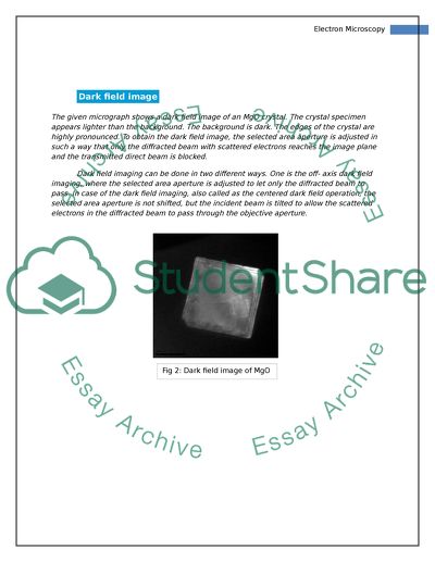
StudentShare
Contact Us
Sign In / Sign Up for FREE
Search
Go to advanced search...
Free

TEM, SEM, EDS in Electron Microscopy - Coursework Example

Cite this document
Summary
This essay analyzes the given micrograph, that shows the selected area diffraction pattern of a MgO crystal. The lattice structure of the crystal is decipherable from the given SAED pattern. Diffraction from a single crystal in a polycrystalline sample can be captured if the aperture is small enough…
Download full paper File format: .doc, available for editing
GRAB THE BEST PAPER93.3% of users find it useful
TEM, SEM, EDS in Electron Microscopy
Read Text Preview

Extract of sample "TEM, SEM, EDS in Electron Microscopy"

You will be provided with a bright field image (Fig a dark field image (Fig. 2) and selected area diffraction pattern (Fig. 7) from the same sample. With the support of ray diagrams explain how the images were obtained. Your explanation must include comments about the location and use of the objective and selected area apertures. Images in TEM are obtained by focusing an electron beam on the specimen. The electrons are absorbed, transmitted, scattered or backscattered. Depending on the kind of image required by the operator, either the transmitted electrons (called direct beam) or the scattered electrons (called diffracted beam) is selected. A selected area aperture is inserted into the back focal plane of the objective lens to select the required beam. When the direct beam is selected, a bright field image is formed, and when the diffracted beam is selected, a dark field image is formed. Bright field image The given micrograph shows a bright field image of an MgO crystal. The crystal specimen appears dark with a bright background. The background appears bright because only the direct beam of transmitted electrons is selected and let to pass through the aperture. The surface topology and the raised texture on top of the crystal are clearly observable. This kind of image is obtained by placing the objective diaphragm or the selected area aperture in the back focal plane of the objective lens. The aperture allows only direct beam to pass through, while blocking the diffracted beam. The direct beam appears as a bright central spot. The aperture also maintains the collection angle. As seen in the ray diagram below, the objective aperture blocks the diffracted beam, allowing only the transmitted beam to reach the image plane. Dark field image The given micrograph shows a dark field image of an MgO crystal. The crystal specimen appears lighter than the background. The background is dark. The edges of the crystal are highly pronounced. To obtain the dark field image, the selected area aperture is adjusted in such a way that only the diffracted beam with scattered electrons reaches the image plane and the transmitted direct beam is blocked. Dark field imaging can be done in two different ways. One is the off- axis dark field imaging, where the selected area aperture is adjusted to let only the diffracted beam to pass. In case of the dark field imaging, also called as the centered dark field operation, the selected area aperture is not shifted, but the incident beam is tilted to allow the scattered electrons in the diffracted beam to pass through the objective aperture. A collective ray diagram for both bright field and dark field imaging is given below: Selected Area Diffraction Pattern The given micrograph shows the selected area diffraction pattern of an MgO crystal. The lattice structure of the crystal is easily decipherable from the given SAED pattern. Diffraction from a single crystal in a polycrystalline sample can be captured if the aperture is small enough and the crystal is large enough. To obtain such a pattern, the selected area aperture is placed in the image plane of objective lens and used to select only one part of the image. Using projector lenses to focus on electron beams to obtain small spots on the object surface, the diffraction patterns can be obtained. Using this pattern, the lattice of crystals can be easily studied and it is also possible to determine the orientation relationships between grains or even different phases. 2. (a) From a lattice image obtained from a single crystal of BaZrO3 (Fig. 4) determine the magnification. Compare this with the magnification obtained using the scale bar. Calculate the length the scale bar should be. To calculate the magnification from the lattice image given, the following formula for magnification is used: Magnification (M) = A stepwise solution for the given problem is presented below: Step 1 Calculation of pixel to cm ratio: The size of the image is measured in pixels and centimeters and found to be: Height in pixels= 556 pixels= 14.7cm Width in pixels= 549 pixels= 14.5 cm The pixel to cm ratio is found to be: Height: 556/14.7=37.8 Width: 549/14.5=37.86 Mean of both the ratios=(37.8+37.86)/2=37.83 Step 2 The number of lattice spacing in a region corresponding to the 20 nm scale bar is estimated. There are 43 lattice spacing in an area equal to 134 pixels or 3.54 cm corresponding to the length of space bar. Therefore, 43 lattice spacing fit into 3.54 cm. from this the image length can be found out for 43 lattice spacing: Image length for 43 lattice spacing=3.54 cm= 3.54?107 nm Step 3 Object length for 43 lattice spacing=0.419?43(given that the lattice spacing of BaZrO3 in the [1,0,0] lattice plane is 0.419 nm) (Yamada et al 2006) Therefore, Object length=0.419?43=18.017nm Step 4 Magnification (M)== = 0.195?107=1.95?106 Therefore, the magnification of the given image is found to be 1.95?106 When this magnification is compared with the magnification found with the scale bar, the following results are obtained: Scale bar=134 pixels=3.54 cm= 3.54?107 nm The scale bar corresponds to 20 nm (given) Magnification= 3.54?107/20=0.177?107 nm=1.77?106 nm Ratio of the two magnifications= 1.95?106/1.77?106=1.10 The scale bar and the magnifications are in agreement. The length of the scale bar should be the same, i.e. 3.54 cm. 2.(b) Explain the fringes present on the circular ZrO2 grain. The fringes on the circular ZrO2 grain are best explained as Moire Fringes. These fringes occur because the ZrO2 grain is embedded in the BaZrO3 crystal and there is lattice mismatch in both the lattices. The difference in lattice spacing of both ZrO2 and BaZrO3 is the cause of such a mismatch, resulting in Moire Fringes. 3.(a) You are provided with images with and without condenser astigmatism (Fig. 5 & 6); explain how this aberration may be reduced. If this aberration is not minimised describe the effect this has on high magnification images. The two micrographs given are of condenser astigmatism. The figure 5, with circular electron beam has no condenser astigmatism, whereas the figure 6 with an elliptical electron beam has condenser astigmatism. How this aberration can be reduced: Condenser astigmatism is a kind of chromatic aberration, where the incident electron beam appears elliptical. The ellipse can be in both X and Y directions of the focus. There are two lenses C1 and C2 provided in the TEM assembly. The aberration can be nullified by adjusting the C2 lens in such a way that the electron beam shifts itself to form a circular image. Condenser astigmatism causes the image to appear elliptical that rotates 90? on both the sides. The aberration can be eliminated by employing a highly elliptical illumination, i.e. the condenser lens stigmators and adjusting focus settings to produce an illumination patch that is very wide in the direction perpendicular to the biprism when the condenser lens is over focused, but relatively narrow in the parallel direction (Volkl et al 1999). The condenser stigmators work by introducing a compensating magnetic field around the electron beam. Effect on high magnification images If there is failure in elimination of condenser lens astigmatism, there will be considerable reduction in image quality and resolution. There is uneven distribution of the electron beam, leading to reduction in the brightness and contrast of the image. Since the image resolution is affected, the image appears blurred and the fine details of the specimen cannot be focused. 3.(b) Compare focussing and removing objective astigmatism by observation of Fresnel fringes vs. observation of the FFT of the image at high and low magnification. No images are supplied for this question, though you may use images from the literature or internet if they are correctly referenced. In order to remove objective astigmatism, a variety of methods are employed, including observation of Fresnel fringes or fast Fourier transforms (FFT) in the image and adjusting the beam and lenses accordingly. Comparison of both the methods: Fresnel fringes appear when the lens is over focused or under focussed. This happens when the electrons diffract along the edges of the sample forming a diffraction pattern with the transmitted electron beam. The correction can be done by observing the colour of the fringe. If the fringe is white, the objective lens is under focused and if the fringe is black, the objective lens is over focused. The degree of astigmatism can be estimated by comparing the symmetry of the fringes. By adjusting the objective lens stigmator, this kind of astigmatism can be eliminated. In comparison to the above method, the FFT method of correction is a little difficult. In this method, first an amorphous material should be found on the specimen sample. The material could be a carbon film, gold granules or any other such substance. Then, the magnification is increased followed by using computer generated fast Fourier transforms to remove the astigmatism. While the method using Fresnel fringes doesn't require any computer software, the FFT method does. Apart from this, the method using Fresnel fringe only uses the fringes caused in the image, the FFT based method is limited by the availability of the amorphous substance on the specimen and the computer software. At high magnification, it is best to observe Fresnel fringes for reducing astigmatism to obtain a near perfect focus. FFT is best at low magnifications, because Fresnel fringes cannot be observed at low magnification. Fresnel fringes Image: (Watt 1997) 3c. Comment on the white fringe surrounding the MgO crystals in Fig. 9. The MgO crystal given in the micrograph is visible under very high magnification. It has a white fringe surrounding it at the edges. This is because of objective lens astigmatism, resulting in the formation of white Fresnel fringes. The objective lens in this case is under focused and can be corrected by adjusting the objective stigmator. 4a. From a polycrystalline ring pattern from gold (Fig. 8) determine the camera length. Assume an electron accelerating potential of 200kV. The given diffraction pattern has five clearly defined rings of varying radii. Such a pattern can be used to calculate the camera length as follows: The equation for camera length can be derived from the equation, d=, where L = camera length, R =radius of ring and ? =wavelength of the electrons The electron acceleration potential is given as 200 kV. Before finding the camera length, it is necessary to calculate the electron wavelength, using the formula: ?= Therefore, ?=6.63?10-34/ v (2?2.0 ?105 ?1.6?10-19?9.11?10-31)=2.7?10-12 m According to miller indices, the rings are indexed as follows: Gold Miller indices (hkl) d-spacing in Angstrom(A) d-spacing in meter (m) (111) 2.355 2.355?10-12 (200) 2.039 2.039?10-12 (220) 1.442 1.442?10-12 (311) 1.236 1.236?10-12 (222) 1.177 1.177?10-12 Each ring's diameter is measured in pixels and their corresponding values in meter and centimeter is calculated. Only the most prominent inner five rings are considered. Ring Diameter (pixels) Radius (pixels) Radius (cm) Radius(m) L = d ? R/? (m) 1st ring 92 46 1.217 0.012 0.01 2nd ring 106 53 1.402 0.014 0.01 3rd ring 152 76 2.01 0.020 0.01 4th ring 176 88 2.32 0.023 0.01 5th ring 228 114 3.01 0.030 0.01 The mean of the calculated values is 0.01m The camera length (L) is 0.01m 4(b) Use the calculated camera length to index the SAED spot pattern in Fig. 7. The SAED spot pattern in figure 7 represents a bcc (body centered cubic crystal) structure. The miller indices are given in the following table: d= The R values are measured in pixels. For example, R1=176 pixels= 4.65 cm= 0.046m The d value for the corresponding R is calculated. For example, for R1, d1=0.01?2.746?10-12/0.046=0.59 This value is equal to miller index (110) Lattice parameter a: We know, d= a/ (h2+K2+l2) 0 .59 ?10-10 = a/ v(12+12+02) a= 0.59 ?10-10 ? 2= 8.3 A d-spacing for all indices: 4(c) From the pattern just indexed determine the zone axis. Taking the vector cross product of any of the two miller indices gives the zone axis: (110) ? (200) = = 0i-0j-2k = (0, 0,-2) Select and compare a SE and BSE image taken from the same region of a sample. 1a. Highlight differences between the two images, referring to specific features in the images. The two micrographs above are the Back scatter electron image and the Secondary electron image of a rock. The differences between the rocks are as follows: The BSE image has greater contrast than the SE image. The SE image appears more 3 dimensional, with greater edge highlighting. The varying composition of the rock sample is more visible in the BSE, with more contrast variation, unlike the SE image. The topology of the SE image is more visible and the details of the specimen are clear, while the BSE image looks flatter. 2b. Using the properties or characteristics of the SE and BSE, explain the observed differences. Clearly state the contrast mechanisms in each image. The reasons for the observed differences in the two images are explained as follows: In case of the BSE image, the high energy electrons formed deep inside the material are backscattered and so the areas of varying compositions form greater contrast than the SE image. In case of SE image, the low energy electrons at the surface of the specimen are captured. That is why it is of low contrast. Since the SE image is formed due to surface electrons, there is greater edge highlighting in the image and it appears more three dimensional. In the BSE image, the high energy electrons that produce back scatter produce varying contrast varying with regions of high atomic number and low atomic number. Regions with higher atomic number produce more backscatter and vice versa, making the varying composition visible. The topology in SE is clearly visible because the regions that are raised produce more secondary electrons, making them visible in the image, while the BSE looks more flat. Images of a tilted TEM grid are provided showing a large difference in depth of field (file names DOF 1, 2, 3). 3 Calculate the depth of field from the images provided. Explain how you arrived at your answer. Compare SEM figures with the depth of field that would be available from an optical microscope for the same magnification. The depth of field for the images given is calculated as follows: In the equation given above, d=SEM minimal resolution, W = Working distance, D = aperture size Here, d=3.5 nm = 3.5 ?10-9 m and D=200?m = 200?10-6 m, W has to be converted to meter from mm by multiplying with 10-3 WD (mm) WD (m) Depth of field (m) Depth of field for first image 13.0 13.0?10-3 4.55?10-7 Depth of field for second image 14.3 14.3?10-3 5?10-7 Depth of field for third image 44.3 44.3?10-3 1.55?10-6 The depth of field of optical microscope would be 1/300 times that of the Scanning electron microscope. Images obtained from a sample at 2, 15 and 30 kV are provided (file names Circuit 1, 2, 3). 4a. Describe differences in the images and explain these differences based on interaction volume changes with kV. The contribution from both SE and BSE must be taken into account. Differences in images obtained at 2, 15 and 30 kV: The image at 2 kV shows very less distinction between the sample and the substrate. The substrate is a little more observable in the image at 15 kV, and even more in the one obtained at 30 kV. The features in the 2 kV image are extremely light and the fine details are almost invisible. The raised circular grains and horizontal lines on substrate are also invisible. The lines are most prominent in the image obtained at 30 kV, and a little lesser in 15 kV. The fine circular grains are most prominent in the image obtained at 15 kV. The image obtained at 2 kV has very low contrast; the one at 30 kV has the highest contrast. The differences given above can be explained as follows: At 2 kV, there are very less secondary electrons and so, the topology of the image is almost invisible. At a higher kV, at 15 kV, there is better resolution and the topology is the clearest. This is because enough secondary electrons are released, making the raised parts visible. At 30 kV, the contrast is highest because there is more backscatter of electrons, and less secondary electrons because they are being re-absorbed into the specimen. Because of the reduced secondary electrons, the topology is less visible. 4b. Estimate the depth of penetration of 2, 15 and 30 kV electrons for the sample used. Using a copper sample and Monte Carlo simulation in Casino v2.42, the depth of penetration at the given keV is estimated as follows: Depth of penetration at 2kV 25.5nm Depth of penetration at 15kV 550 nm Depth of penetration at 30kV 1811.1nm Compare the high resolution images ‘Gold on carbon.jpg’ (FE-SEM image) and ‘Gold on carbon2.jpg’ (tungsten filament SEM image). 5a List all the instrument parameters used to capture the tungsten filament SEM image and explain why the selected instrument conditions were used. To obtain the tungsten filament SEM image, a thermionic emission source, i.e. a tungsten filament is used. It has the highest melting point and the lowest vapour pressure among all metals. It is heated by passing electric current through it till the heat is enough to overcome the work function of the metal to emit electrons. The diameter of the filament should be 100 micrometers and the optimum filament temperature for thermionic emission of electrons is around 2700 degrees Kelvin. The accelerating voltage is generally between -500 Volts and -50,000 Volts DC... Electrons leaving the filament will be accelerated along the gradient towards the most positive area, the anode. This beam of electrons will be focused by the shape of the field gradient to a cross-over just before the anode, forming the first optical image of the source and ensuring that a larger percentage of the electrons will pass through the aperture of the anode (Sampson 1996). Here are its characteristics: •Thermal emitter •Low brightness •Spot size: ~4.0 nm •Resolution: 4.0 nm at 30 Kv (Sen) 5b Explain why different conditions were used for the FE-SEM image and comment on the benefits of field emission sources. Note: An inlens detector is a secondary electron detector located inside the pole piece. An FE SEM or the field emission SEM is obtained strictly under vacuum conditions. The filament (a sharp pointed tungsten filament) in the FE SEM is not directly heated and is place in an electric potential gradient instead. The electrical field produced is concentrated to a very high range. The electrons should thus be released when the work function of tungsten is lowered. This is affected when absorbed gases are present in the area of operation. This is the prime reason for using high vacuum. . This also prevents excessive electron scattering. The benefits of field emission sources are given below: Compared to the images obtained using a tungsten filament, the images obtained from FE SEM are clearer. The possible magnification and resolution is higher. FESEM uses Field Emission Gun producing a cleaner image, less electrostatic distortions and spatial resolution < 2nm (that means 3 or 6 times better than SEM) (Polytechnic of Turin) FESEM produces clearer, less electrostatically distorted images with spatial resolution down to 1 1/2 nm. That's 3 to 6 times better than conventional SEM. Smaller-area contamination spots can be examined at electron accelerating voltages compatible with Energy Dispersive X-ray Spectroscopy. Reduced penetration of low kinetic energy electrons probes closer to the immediate material surface. High quality, low voltage images are obtained with negligible electrical charging of samples. (Accelerating voltages range from 0.5 to 30 kV). Need for placing conducting coatings on insulating materials is virtually eliminated. For ultra-high magnification imaging, inlens FESEM can be used (Photometrics.net). Compare figures ‘Pollen 1, 2 & 3’. 6a. Explain the benefits of using a mixed signal image. As is evident from the given micrographs of pollen grains, the image with a mixed signal gives a better idea of both the topology, composition and the finer details of the specimen. This is because it combines the advantages of both SE and BSE. The edge highlighting that is present in SE is also eliminated. 6b. Explain what image averaging and image integration is. How do these noise reduction methods improve a SEM image? An image gets distorted due to the presence of noise which can be due to the presence of scattered secondary electrons, gray level fluctuations occurring because of electrostatic charges, improper alignment of the target specimen region, electron beam and the secondary electron detector. The noise in SEM is also because of background clutter. In order to eliminate distortions caused by these noise sources various noise reduction methods like image averaging and image integration are used. The image averaging involves averaging the images to give an average first image and an average second image that are then correlated. This technique is used to remove random noise. Several consecutive images are taken and then averaged. "The principle is that if the scene is completely still without any subject movement, the only variable between the identically exposed frames will be the random noise. Averaging the frames removes this noise (Freeman 2008). The image integration technique involves the averaging of a series of images over a period of time, where the only variable is time. The images are then integrated using computer software. Any random noise can be easily removed. How these noise reduction methods help in improving the SEM image: The distortion of the image because of noise lowers the resolution and high definition images cannot be obtained. Moreover, because of the random noise, the finer details of the specimen cannot be studied. When such image reduction techniques are used, the quality of the image is increased and the finer details can be properly studied. It is becomes possible to obtain high definition images. Use appropriate images from the portfolio to answer the following; 7a. Explain what sample charging is. Explain methods to reduce charging. Sample charging is a phenomenon that occurs because of a build up of charge on the surface of the sample on bombardment with electrons. When an electron beam is incident on a sample, secondary electrons and backscattered electrons are produced. But in some cases, instead of passing through or scattering, the electrons are deflected randomly because of the electric field generated because of charge build up on the specimen. Therefore, we get varying bright zones and lines of the image screen randomly, distorting the image. Sample charging can manifest itself in the form of bright lines on the image, called line by line charging, or the entire screen area appears bright or dark, called general charging, or only the edges of the specimen appear extremely bright, called edge charging. Sometimes, charging can result because of electrons left over in a previous SEM operation and cause residual charging. Given below are methods to reduce charging: Sample charging can be eliminated by using any method that reduces the build up of charge on the sample surface. This can be done by accelerating voltage, increasing scan rate so that the sample is exposed to electron beam for a very small amount of time, reducing the spot size to limit the amount of electrons hitting the sample, or coating the sample with gold or any other conductive layer. It is shown that a focused ion beam (FIB) grounding technique can be used to alleviate charge build up on samples that would otherwise charge in the electron beam (Gondran and Morales 2006). 7b. Explain methods/approaches that can be used to eliminate or reduce edge highlighting. Edge highlighting occurs when more secondary electrons are detected from the raised surfaces. Many attempts have been made to reduce edge highlighting. According to V. N. Robinson, construction of an efficient geometric backscattered electron detector will be able to eliminate edge highlighting. " This detector appears to have approximately the same limit of spatial detectability as a secondary electron detector. It has the advantages over a secondary electron detector of a reduction of charging artifacts, improved flat surface contrast and reduced edge highlighting (Robinson 1974). Using Atomic number contrast imaging can also reduce edge highlighting (Johari 1979). This kind of imaging depends on the relationship between BSE emission characteristics and the sample composition. 7c. Explain why figure ‘Geopolymer 2’ exhibits less charging than ‘Geopolymer 1’ given the SEM operating conditions are the same. Note: figure ‘Geopolymer 1’ was collected with a slow scan rate and figure ‘Geopolymer 2’ was collected with a fast scan rate and a 120 frame average. The geo polymer image taken at a slow scan rate shows more charging than the image taken at a higher scan rate (at a 120 frame average), though the SEM operating conditions were the same. This is because the amount of time the sample was exposed to the incident electron beam was very less because of high scan rate for the second image. Because of the less exposure time, there was no time for charge build up on the specimen surface. Inversely, in case of the first image, when the image was taken at a slow scan rate, the electron beam was incident on the sample for a longer time, leading to charge build up, causing sample charging. You will be provided with x-ray spectra collected from copper at 5, 10 and 20 keV. 1a. Measure the L/K ratio, resolution, zero point and gain from the copper spectra. The given X-ray spectra are plotted in WinPLOTR to obtain the following peaks: Calculation of the L/K ratio: Energy (keV) K energy (keV) K int. (counts) K FWHM (keV) L energy (keV) L int. (counts) L FWHM (keV) L/K Background (Counts) 5 0.934 1126 0.081 - - - - 28.12 10 0.932 2837 0.078 8.038 25.8 0.167 0.0091 45.84 20 0.929 6428 0.081 8.037 1947 0.154 0.3029 66.27 Calculation of resolution: Smallest value of FWHM is resolution Resolution for 5 keV 0.081 Resolution for 10 keV 0.167 Resolution for 20 keV 0.154 Calculation of gain: Gain for 5 keV 1126/28.12 40.04 Gain for 10 keV 2837/45.84 61.88 Gain for 20 keV 6428/66.27 96.99 1b. Explain the variation in L/K ratio just measured. Indicate the relative importance for each reason provided. As the keV is increasing, the L/K ratio is also increasing. At 5 keV, both the L and K peaks are almost invisible or absent. The voltage is lesser than the cut off voltage required for excitation of electrons for generation of peaks. At 10 keV, the L peak is still invisible, but the K peak is considerably high. The voltage is quite near the cut off voltage so that some of the electrons are excited, leading to a higher peak. At 20 keV, both L and K peaks are high as the voltage is higher than the cut off voltage for excitation of electrons. The importance of this observation is that accurate spectral analysis can be done at higher voltages. A BSE image from a sample with regions of different average atomic number will be provided. In addition, selected x-ray maps and spot mode spectra from the same area will be made available. 2 Discuss the relative merits of the BSE image, x-ray maps and spot mode spectra. The given images are of a mineral that is observed in X-ray and spot mode spectra. Merits of using BSE, X-Ray maps and spot mode spectra are given below: Using BSE, it is possible to visualize and detect the varying compositions of the sample, but the exact elemental composition of the sample cannot be estimated. However, it is faster than X-ray mapping. The X-ray making can be done to get a map of the different elemental compositions of the sample and the distribution across the specimen. It is slower but useful. Once an X-ray map is obtained, using the spot mode, a specific area can be further analysed to find out the exact elemental composition of that region using spectral analysis. In case of the given image, the exact composition of the given sample is estimated to be carbon, oxygen, silicon, chlorine, copper and silver. This method is of high utility in finding the exact composition but is slower. Bibliography Andrade, R. FFT Measurements. Federal University of Minas Gerais. http://imagej.nih.gov/ij/docs/examples/tem/ (accessed June 1, 2011). Freeman, M. The Complete Guide to Night & Lowlight Digital Photography. New York: Sterling Publishing Company, Inc., 2008. Gondran, C. F.H., Emily Morales. "Focused Ion Beam Grounding to Alleviate Sample Charging for Scanning Auger Electron Spectroscopy". Proceedings of the 32nd International Symposium for Testing and failure analysis, USA, 2006. Johari, O. Scanning electron microscopy. Scanning Electron Microscopy, Inc, 1979. PhotoMetrics, Inc. "Field Emission: Scanning Electron Microscopy (FESEM)". http://www.photometrics. net/fesem.html (accessed June 1, 2011). Robinson, V. N. E. "The construction and uses of an efficient backscattered electron detector for scanning electron microscopy", Journal of Physics E: Scientific Instruments 7 (1974): 650, doi: 10.1088/0022-3735/7/8/019. Sampson, Allen R. "Scanning Electron Microscopy". Advanced Research Systems. http:// advressys.com /analytic/sem.htm (accessed June 1, 2011). Sen, S. "Scanning Electron Microscopy in Imaging and Analytical Modes". CGCRI. http://www.scribd.com/doc/ 13729635/Sem-1 (accessed June 1, 2011). Volkl, E., Lawrence F. Allard, David C. Joy. Introduction to Electron Holography. New York: Springer, 1999. Watt, Ian M. The principles and practice of electron microscopy. London: Cambridge University Press, 1997. Williams, D. B., and C. B. Carter. Transmission electron microscopy: a textbook for materials science. New York: Springer, 2009. Yamada, K., A. Ichinose, Y. Shingai, K. Matsumoto, Y. Yoshida, S. Horii, R. Kita, S. Toh, K. Kaneko, N. Mori, M. Mukaida, "TEM observation of ErBa2Cu3O7-[delta] films with BaZrO3 artificial pinning centers", Advanced Superconductivity 18 (2006): 660-66, doi: 10.1143/JJAP.47.899 Read More
Cite this document
  • APA
  • MLA
  • CHICAGO
(“TEM, SEM, EDS in Electron Microscopy Coursework - 1”, n.d.)
Retrieved from https://studentshare.org/physics/1424047-electron-microscopy
(TEM, SEM, EDS in Electron Microscopy Coursework - 1)
https://studentshare.org/physics/1424047-electron-microscopy.
“TEM, SEM, EDS in Electron Microscopy Coursework - 1”, n.d. https://studentshare.org/physics/1424047-electron-microscopy.
  • Cited: 0 times

CHECK THESE SAMPLES OF TEM, SEM, EDS in Electron Microscopy

Scanning Electron Microscope

In the subsequent sections interaction of electrons with matter, basic principles of electron microscopy, architecture and working of scanning electron microscope, different attachments to an SEM and applications of SEM in materials science will be discussed in brief with special emphasis on specifications of a modern SEM.... Scanning electron Microscope (SEM): A Diverse Analytical Instrument Introduction Scanning electron microscope (SEM) is among the most versatile analytical instruments available to materials scientists....
7 Pages (1750 words) Essay

Surface Analysis and Materials Science

Table 1 Most Commonly Used Surface Analysis Methods Incident Excitation Probe photon electron ion neutron electric/magnetic field Radiation Detected photon FTIR, Raman, XAFS, EXAFS, SFG, IR EDAX NRA GDOES electron XPS/ESCA, UPS, (AE) XAFS AES, SAM, SEM, TEM, LEED, RHEED, SPE, STM, EELS STM, AFM ion SIMS, LEIS, RBS, ISS neutron INS As shown in Table 1, the following shows the most commonly used surface analysis methods: FTIR – Fourier Transform Infrared Spectroscopy; Raman Vibrational Spectroscopy; XAFS – X-ray Absorption Fine Structure analysis; EXAFS – Extended X-ray Absorption Fine Structure analysis; SFG – Sum Frequency Generation; IR – Infrared Spectroscopy; EDAX – Energy Dispersive Analysis of X-rays; NRA – Nuclear Reaction Analysis; GDOES – Glow Discharge Optical Emission Spectroscopy; XPS/ESCA – X-ray Photoelectron Spectroscopy / Electron Spectroscopy for Chemical Analysis; UPS – Ultraviolet Photoelectron Spectroscopy; (AE) XAFS – Auger Emission X-ray Absorption Fine Structure analysis; AES – Auger Electron Spectroscopy; SAM –Scanning Auger Spectroscopy; SEM – Scanning electron microscopy; TEM – Transmission electron microscopy; LEED – Low Energy Electron Diffraction; RHEED – Reflection High Energy Electron Diffraction; SPE – Spin Polarized Electron spectroscopy; STM – Scanning Tunnelling Microscopy; EELS – Electron Energy Loss Spectroscopy; AFM – Atomic Force Microscopy; SIMS – Secondary Ion Mass Spectrometry; LEIS – Low Energy Ion Scattering spectroscopy; RBS – Rutherford Backscattering Spectroscopy; ISS – Ion Scattering Spectroscopy; and INS – Inelastic Neutron Scattering; Analysis Auger electron spectroscopy or AES is considered as a key chemical surface analysis tool for conducting material samples....
7 Pages (1750 words) Essay

Powder Characterization by SEM, SEM-EDAX, and TEM

Besides, many attributes like shape and chemistry can be determined only by advanced electron microscopy.... However, only a direct method like microscopy gives confidence in the result.... lectron microscopy involves obtaining high magnification images of the samples using a focused beam of accelerated electrons as a probe and then forming images by collecting the different signals like backscattered electrons, secondary electrons, transmitted electrons, etc [1]....
7 Pages (1750 words) Essay

Scanning Electron Microscope Operation

Areas that range from a width of one centimetre to as minute as five microns can be seen in scanning mode using techniques in scanning electron microscopy.... Scanning electron Microscope Instructor: Scanning electron Microscope The scanning electron microscope utilizes a beam of focused high-energy electrons for the generation of various signals on the surface of specimens (Reimer, 2008 p97).... hellip; The signals derived from the interaction between the sample and the electron reveals information regarding the sample inclusive of texture, material orientation in the sample, crystalline structure, and chemical composition....
6 Pages (1500 words) Essay

Use of the scanning electron microscopy in the food industry

Use of the scanning electron microscopy in the food industry.... … Scanning electron microscopy (SEM), as well as other techniques such as energy dispersive spectroscopy (EDS) is an effective tool used for the identification and characterization of particulate contamination and foreign body contamination of food.... This paper will examine the use of scanning electron microscopy in the food industry discussing its effectiveness in detecting and identifying foreign bodies in food compounds and products....
6 Pages (1500 words) Research Paper

Surface Analysis

This paper presents Surface Analysis which is a nondestructive method of testing used to analyze the chemical and molecular composition of different surfaces depending upon its use.... This method uses the simple principle of pounding a sample specimen with electrons, x rays or photons.... hellip; As the study highlights, in this process, the surface of the sample is subjected to a steady stream of focussed primary ions....
7 Pages (1750 words) Assignment

Scanning Electron Microscope

Sizes that range from a width of one centimetre to as minute as five microns can be seen in scanning mode using scanning electron microscopy techniques.... This papper ''Scanning electron Microscope'' tells that The scanning electron microscope utilizes a beam of focused, high-energy electrons to generate various signals on the surface of specimens.... The signals derived from the interaction between the sample and the electron reveal information regarding the selection etc....
6 Pages (1500 words) Article

Use of the Scanning Electron Microscopy in the Food Industry

This term paper "Use of the Scanning electron microscopy in the Food Industry" examines the use of scanning electron microscopy in the food industry discussing its effectiveness in detecting and identifying foreign bodies in food compounds and products.... hellip; Scanning electron microscopy (SEM), as well as other techniques such as energy dispersive spectroscopy (EDS), is an effective tool used for the identification and characterization of particulate contamination and foreign body contamination of food....
6 Pages (1500 words) Term Paper
sponsored ads
We use cookies to create the best experience for you. Keep on browsing if you are OK with that, or find out how to manage cookies.
Contact Us